Overview
Femtosecond laser direct writing (FLDW) enables fabrication of optical waveguides and photonic circuits deep inside transparent glass through permanent refractive index modification. This non-contact, single-step technique produces complex 3D photonic devices impossible to achieve with planar lithography. Applications span integrated photonics for communication, quantum information processing, astrophotonics, and lab-on-chip biosensing.
Physical Principle
Tightly focused femtosecond pulses induce multiphoton absorption in the focal volume (~1 μm³), triggering local densification or microexplosion depending on pulse energy. This creates a permanent refractive index change (Δn ≈ 10⁻⁴ to 10⁻²) in glass. Three-dimensional fabrication is achieved by translating the sample relative to the fixed focal point. Unlike surface processing, the beam transmits through bulk glass until reaching the focal plane, enabling writing at depths from micrometers to centimeters.
Recommended CP-Series Models for This Process
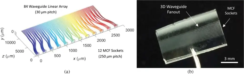
Femtosecond laser-written photonic circuits in glass. (a) 84-waveguide linear array (30 μm pitch) demonstrating high uniformity over 3 mm chip width, with 12 MCF (multi-core fiber) sockets at 250 μm pitch for fiber-chip coupling. (b) 3D waveguide fanout structure showing vertical routing capability: waveguides transition from compact 30 μm spacing to expanded 250 μm MCF socket spacing through 3D spatial distribution. This geometry is impossible with planar lithography. Reproduced from Tan et al., Adv. Photonics 3(2), 024002 (2021). © 2021 The Authors. Published by SPIE under open access license.
Technical Capabilities
Compatible Materials
Fused Silica (SiO₂)
Lowest loss (0.2 dB/cm), highest Δn, telecom applications
Borosilicate Glass (BK7, Eagle XG)
Cost-effective, good optical quality, displays
Phosphate Glass
High rare-earth solubility for amplifiers
Chalcogenide Glass (As₂S₃)
Mid-IR transparency, nonlinear optics
Sapphire (Al₂O₃)
Extreme environments, high-temp sensing
Applications
Integrated Photonics for Communication
- •Fiber-to-chip couplers (3D fanout geometries)
- •Wavelength multiplexers/demultiplexers
- •Directional couplers and beam splitters
- •Arrayed waveguide gratings (AWG)
Quantum Information Processing
- •Multi-path interferometers for quantum gates
- •Entangled photon sources (waveguide-integrated SPDC)
- •Boson sampling circuits
- •Single-photon detectors integration
Astrophotonics
- •Stellar interferometry beam combiners
- •Fiber Bragg gratings for wavelength references
- •Photonic lanterns (single-mode to multi-mode conversion)
- •Astronomical spectrographs
Lab-on-Chip & Biosensing
- •Optofluidic waveguides (light confinement in liquid-core channels)
- •Evanescent wave biosensors
- •Fluorescence-based microfluidic detection
- •Integrated absorption spectroscopy
Technology Comparison
| Parameter | Femtosecond Laser Writing (3D) | Ion Exchange (2D) | Planar Lithography (2.5D) |
|---|---|---|---|
| 3D Routing | True 3D arbitrary paths | Surface only | Stacked 2D layers |
| Propagation Loss @ 1550nm | 0.2-1 dB/cm | 0.1-0.5 dB/cm | 0.01-0.1 dB/cm |
| Coupling Loss to SMF | 0.1-0.4 dB/facet | 0.5-2 dB/facet | 0.1-0.5 dB/facet |
| Fabrication Time | Hours (rapid prototyping) | Days (diffusion process) | Weeks (multi-mask) |
| Design Iteration | Direct CAD-to-device | Mask redesign | Full re-fabrication |
| Equipment Cost | Moderate (laser + stages) | Low | Very high (cleanroom) |
Related Application Spotlight
Ready to Implement This Process?
Contact us to discuss rental options (from €5000/month), outright purchase, or to connect with our partner network for job shop processing and process development services (paid).