Application Spotlight: Femtosecond SERS Nanostructures in Glass - From Surface Patches to Buried Microchannels
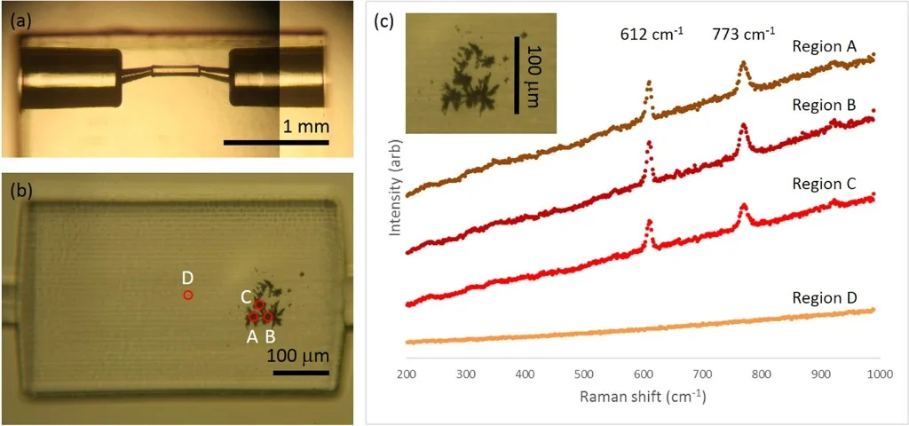
A Scientific Reports publication demonstrates a practical femtosecond workflow for writing silver nanoparticle (AgNP) SERS regions directly on fused silica, with a major extension: the same approach can be moved into buried microfluidic channels inside glass.
Not Only SERS Substrates - Also 3D Microfluidic Integration
This work is especially relevant for engineering teams building compact sensing systems. The paper shows two capabilities in one process family:
- Surface SERS regions: laser photoreduction of Ag+ precursors creates dense AgNP areas for strong Raman enhancement.
- In-channel SERS monitors: AgNPs are inscribed on the inner wall of a buried microchannel in fused silica, enabling monolithic optofluidic sensing.
Upcoming Event
Clear Photon will also discuss related spectroscopy and ultrafast processing topics at the upcoming Optica webinar: Spectroscopy for Life Science (Optica).
Core Process Window
The authors used a 1047 nm, 350 fs source and optimized a multi-scan strategy. A key finding was that single-scan patterns are patchy, while repeated scanning substantially improves coverage and signal consistency.
- Best-performing recipe in this study: 5 mW writing power, 0.02 mm/s scan speed, 400 scans
- Resulting nanostructure scale: disordered connected Ag nanospheres around 50 nm
- Peak analytical enhancement: up to approximately 1.4 × 10¹¹
Why It Matters for Device Teams
Traditional SERS microfluidics often require separate substrate preparation and bonding steps. Here, the same ultrafast platform can fabricate the channel architecture and then write the SERS-active region where needed. That reduces assembly complexity and supports rapid prototyping of custom sensing geometries.
For Clear Photon users, this is a strong example of how femtosecond systems can bridge materials processing, microfabrication, and spectroscopy-grade functionality in a single toolchain.
Related Process Paths
If you are evaluating similar builds, see Ablation, Functional Surface Structuring, and BYOL Laser Integration for practical implementation routes.
Reference: MacKenzie, M.; Chi, H.; Varma, M.; Pal, P.; Kar, A.; Paterson, L. "Femtosecond laser fabrication of silver nanostructures on glass for surface enhanced Raman spectroscopy." Scientific Reports 2019, 9, 17058. DOI: 10.1038/s41598-019-53328-6. Open access under CC BY 4.0.
Interested in This Application?
Contact us to learn how Clear Photon workstations can enable your research or production process.
Get in Touch