Application Spotlight: Femtosecond Laser Additive Manufacturing – The Next Generation of 3D Metal Printing
A comprehensive review published in Quantum Beam Science examines femtosecond laser-based additive manufacturing (AM), demonstrating capabilities that address fundamental limitations of conventional continuous-wave (CW) and long-pulsed laser powder bed fusion technologies.
Industrial Context
Metal additive manufacturing has achieved industrial adoption across aerospace and automotive sectors. GE Aviation employs AM-produced nozzles in LEAP engines, reducing part count from 20 to 5 while increasing durability fivefold. Boeing incorporates over 70,000 AM parts across its programs.
However, conventional laser-based AM faces technical limitations:
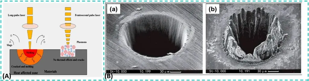
- Heat-affected zones (HAZs): CW and long-pulsed lasers produce thermal diffusion beyond the irradiated region
- Microstructural defects: HAZs generate micro-cracks, porosity, and residual stresses that degrade material strength
- Material processing constraints: Ceramics and refractory metals with high melting points remain difficult to process due to thermal management challenges
- Resolution limits: Thermal spread constrains achievable feature sizes
Femtosecond Laser Processing Mechanisms
Femtosecond lasers operate in a fundamentally different processing regime:
- Pulse duration: 10⁻¹⁵ second duration, shorter than the material's heat diffusion time
- Energy delivery: Rapid localized heating (~6000°C) occurs faster than plasma expansion time (ns to μs)
- Heat-affected zone: Limited thermal diffusion produces minimal HAZ (<5 μm for metals)
- Peak power: High instantaneous power enables processing of high-reflectivity and high-thermal-conductivity materials
The underlying physics: electron gas absorbs laser energy and heats in <100 fs, while the lattice heats with a delay of 1-100 ps. Material ablates in tens of ps after absorption, before significant thermal diffusion to surrounding material occurs.
Copper & Silver Nanoparticle Sintering
Copper and silver nanoparticle sintering demonstrates fs laser AM capabilities for flexible electronics fabrication.
Copper Nanoparticle Direct Writing:
- Substrate compatibility: CuO nanoparticles reductively sintered on PDMS and glass
- Feature size: Line widths 10-20 μm achieved through scan speed optimization
- Applications: Temperature sensors, electrodes, flexible circuits on polymer substrates
Silver Nanoparticle Processing (Ti:sapphire, 800 nm, 50 fs, 1 kHz):
- Thermal confinement: Thermal diffusion suppressed to laser focal spot diameter
- Process window: Fluence 30 mJ/cm², effective pulse number 1000
- Microstructure evolution: Solid-state diffusion creates 12 nm interparticle necks at 20 mJ/cm², expanding to 36 nm at 90 mJ/cm²
- Electrical properties: Sheet resistance minimized at optimal fluence before onset of complete particle melting
- Adhesion mechanism: Ag NPs embed approximately half-particle-depth into PET substrate at 90 mJ/cm², increasing contact area
Comparative performance: Fs laser sintering achieved higher electrical conductivity and lower substrate damage than nanosecond laser sintering. AFM analysis showed ns laser created 1.2 μm wide × 500 nm deep affected regions, while fs laser produced 200 nm wide × 90 nm deep regions.
Refractory Metal Processing: Iron & Tungsten
Femtosecond lasers enable additive manufacturing of extremely high-melting-point metals.
Tungsten 3D Printing (melting point 3422°C):
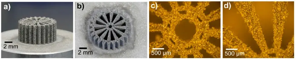
- Demonstrated geometries: Gears (½ inch diameter), 100 μm thin walls, features with integrated holes
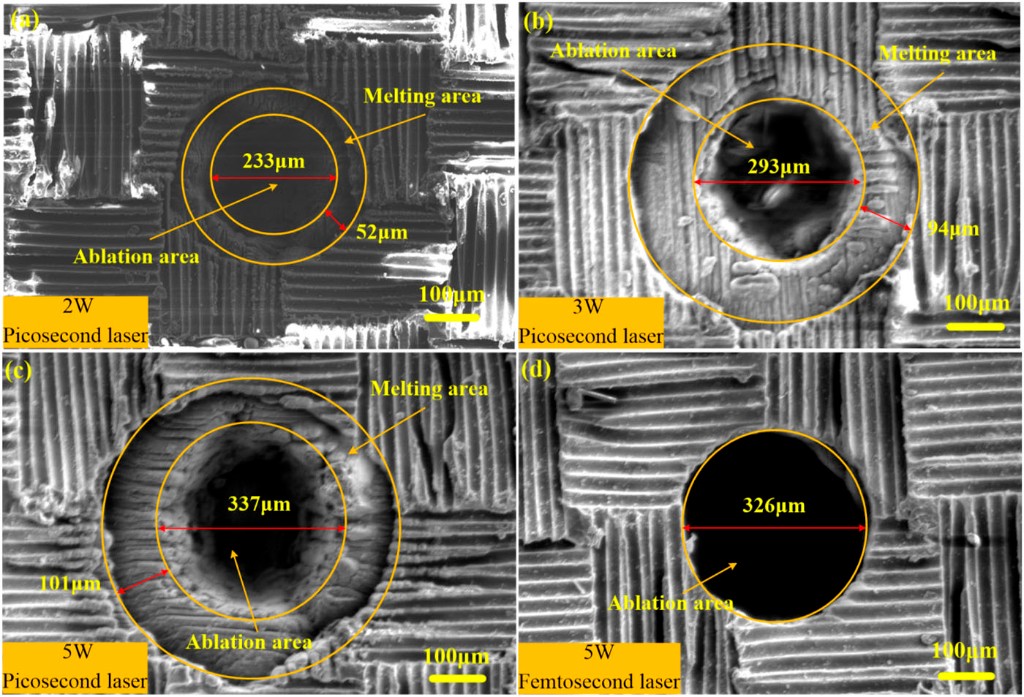
- Grain refinement: Comparative study (fs vs. 20 ps vs. 200 ps vs. CW) showed fs laser produces smallest average grain area
- Mechanical properties: Microhardness measurements showed highest values for fs laser processed samples
- Defect density: Reduced cracks and defects compared to longer-pulse laser sintering
Iron-on-Glass Sintering:
- Technical challenge: Glass brittleness and thermal expansion coefficient mismatch between iron and glass
- Process parameters: 37 W average power, 40 μm layer thickness, 20 μm line spacing, variable scanning speeds
- Optical properties: <1% reflectance achieved for stray light reduction applications
- Substrate integrity: Glass prone to breaking at lower scanning speeds; higher speeds preserved substrate
Aluminum Alloy Processing
Femtosecond laser AM enables processing of challenging aluminum alloys for lightweight aerospace structures.
Al-Li Binary Alloys (High-Lithium Content):
- Conventional casting limit: 2 wt.% Li maximum due to brittle δ-Al-Li phase precipitation
- Fs laser processing: Up to 4 wt.% Li achieved using 500 fs pulses at 20 MHz repetition rate
- Mechanism: High cooling rate in melt pool suppresses excessive Li evaporation during sintering
- Mechanical properties: Significant increase in Young's modulus and decrease in density with increasing Li content
- Process parameters: Pulse energy 1.5 μJ, scanning speeds 0.2-0.7 m/s, layer thickness 40 μm, hatch spacing 30 μm
- Demonstrated components: Complex gear wheels fabricated at 0.7 m/s scanning speed
AlSi40 Hypereutectic Alloy (1030 nm, 500 fs, 20 MHz, 30 W):
- Material composition: 40 wt.% Si in aluminum matrix
- CW laser limitation: Low cooling rates cause Si decomposition due to low Si solubility in Al; minimum achievable track width 150 μm
- Single pulse ablation threshold: 0.12 J/cm² at 1030 nm wavelength
- Processing constraints: Layer thickness 30 μm; fluence >0.13 J/cm² blasts powder from substrate
- Optimal energy range: 40-170 J/m energy per unit length (12-25 W laser power)
- Track quality: Lower scanning speeds (<120 mm/s, >210 J/m) produce melt warps and extensive HAZ with 150-250 μm line widths; higher speeds (>800 mm/s, <30 J/m) form irregular tracks with droplets
- 3D structures: 8 mm diameter, 120 layers × 30 μm layer thickness, 100 μm final wall thickness
- Process atmosphere: Nitrogen gas environment with <0.5% oxygen concentration to prevent oxidation
Al-40Si Comparative Study (fs vs. ps vs. CW):
- Laser systems: 500 fs, 20 ps, and 800 ps pulsed lasers at 1030 nm vs. CW laser at 1070 nm
- Melt pool width: 500 fs and 20 ps at 20 MHz produced smallest width (70 μm) Microhardness: Enhanced hardness with ultrashort pulses vs. CW laser
- Aspect ratio: Depth-to-width ratio increases for shorter pulse duration
- Power threshold: Stable melt pool formation requires >10 W average power and >1 MHz repetition rate
- Ablation onset: Fluence >0.4 J/cm² produces excessive ablation
Multi-Material Layered Structures: Solid Oxide Fuel Cells
Femtosecond laser AM enables single-step fabrication of complex multi-layer electrochemical devices.
SOFC Layer-by-Layer Fabrication (Yb-doped fiber, 1030 nm, 800 fs, 80 MHz, 250 W):
- Traditional fabrication methods: CVD, tape casting, EPD require multiple processing steps, have minimum layer thickness limitations (>10 μm), and involve high equipment costs
- Fs laser approach: Single-step layer-by-layer sintering without binders or post-processing heat treatment
- Device structure: Ni-YSZ anode support layer + YSZ electrolyte layer + LSM cathode layer
- Optimal parameters: 300 mm/s scanning speed, 130 W laser power for high-density Ni-YSZ support layer
- Electrolyte formation: YSZ ink type showed better uniformity than powder spreading; clear melting and fusion to anode base achieved
- Manufacturing advantages: Reproducibility, design flexibility, and component durability in single manufacturing process
Biomedical Applications: Hard Tissue Engineering
Femtosecond laser sintering enables processing of biocompatible ceramics for bone grafting and dental restoration while preserving adjacent soft tissue.
Calcium Phosphate Ceramic Sintering (1045 nm, 100 fs):
- Materials: Fe³⁺-doped brushite (CaHPO₄·2H₂O) and Fe³⁺-doped hydroxyapatite (Ca₁₀(PO₄)₆(OH)₂)
- Thermal profile: 1000°C temperature rise localized to 30 μm diameter irradiation zone
- Thermal decay: Temperature declines to 40°C within 500 μm radial distance
- Soft tissue safety: Tissues located >500 μm from irradiation zone experience no thermal damage
- Phase transformations: Fe³⁺-doped brushite transforms to β-calcium pyrophosphate; Fe³⁺-doped HAP transforms to calcium-iron-phosphate
- Doping effect: 10% Fe³⁺ doping improves laser absorption and enables microstructural sintering and densification
- Applications: Highly porous calcium pyrophosphate for bone regeneration scaffolds and coatings; dense calcium-iron-phosphate layer for acid-eroded enamel restoration and small bone defect treatment
Process Parameter Dependencies
Critical parameters for fs laser additive manufacturing:
- Pulse duration: 100-800 fs range demonstrated across different material systems
- Repetition rate: 1 kHz to 80 MHz depending on material and thermal accumulation requirements
- Average power: 10-250 W determined by material properties and desired processing speed
- Scanning speed: 0.1 mm/s to 1 m/s range depending on required resolution and throughput
- Layer thickness: 15-50 μm typical for powder bed fusion processes
- Hatch spacing: 10-30 μm for adequate inter-track bonding
- Atmosphere control: Nitrogen or vacuum environment to prevent oxidation during processing
Comparative Performance: Ultrashort vs. Long-Pulse Lasers
Documented advantages of femtosecond laser AM over CW and long-pulsed systems:
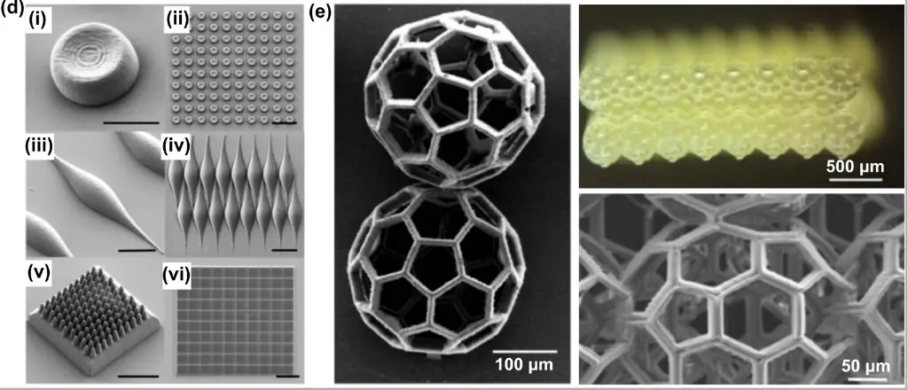
- Increased part resolution through confined thermal zones
- Rapid cooling rates minimize grain growth
- Reduced residual stresses due to minimal thermal gradients
- Reduced oxidation from short laser-matter interaction times
- Lower substrate damage through confined heat-affected zones
- Improved wettability from localized melting
- Capability to process dielectrics and ceramics via multi-photon absorption
Market Projections & Application Sectors
The global ultrafast laser market is projected to reach USD 3.31 billion by 2026 with a compound annual growth rate of 16.6% between 2021 and 2026. Despite high initial capital investment, the precision manufacturing capabilities justify deployment in:
- Aerospace: Complex lightweight geometries, high-strength alloys, rapid prototyping
- Biomedical: Patient-specific implants, dental restoration devices, tissue engineering scaffolds
- Electronics: Flexible conductive circuits, SERS substrates for molecular detection, microelectrode arrays
- Automotive: Lightweight structural components, dissimilar material joining, rapid tooling
- Energy: Fuel cell electrode structures, battery components, catalyst supports
- Defense: Custom components, refractory metal parts, field-deployable manufacturing
Technical Challenges & Research Directions
Current limitations:
- Heat accumulation effects at very high repetition rates (>10 MHz) requiring thermal management strategies
- Material-specific process parameter optimization requiring extensive experimental investigation
- Transition from laboratory-scale demonstrations to production-scale implementation
- Integration with existing AM quality control and process monitoring systems
Future research opportunities:
- Desktop fs laser AM systems with integrated Class 1 safety enclosures for standard laboratory deployment
- Multi-beam architectures for increased throughput
- Real-time process monitoring with closed-loop parameter control
- Hybrid manufacturing combining fs laser processing with conventional AM techniques
- Expansion of processable materials to include advanced ceramics, metal-matrix composites, and functionally graded materials
As femtosecond laser technology matures and system costs decrease, desktop workstations are bringing precision metal and ceramic additive manufacturing capabilities into standard R&D laboratories, eliminating requirements for dedicated laser safety rooms and specialized operator training.
Reference: Kaligar, A.B., et al. "Femtosecond Laser-Based Additive Manufacturing: Current Status and Perspectives." Quantum Beam Science 2022, 6(1), 5. https://doi.org/10.3390/qubs6010005
Interested in This Application?
Contact us to learn how Clear Photon workstations can enable your research or production process.
Get in Touch