Application Spotlight: Stealth Dicing of Sapphire with Femtosecond Bessel Beam – Zero Kerf, Zero Taper, 200 nm Surface Finish
Research published in Optics & Laser Technology demonstrates a breakthrough sapphire cutting method using femtosecond Bessel beam stealth dicing, achieving 200 nm Ra surface roughness, nearly an order of magnitude improvement over previous laser Bessel beam approaches, with zero kerf width, zero taper, and crack-free cutting suitable for LED substrate manufacturing.
The Sapphire Cutting Challenge
Sapphire (α-Al₂O₃) combines extraordinary properties with extreme processing difficulty:
Material Properties:
- Hardness: Mohs 9.0 (second only to diamond at 10.0)
- Optical transmissivity: 0.15-5.5 μm wavelength range
- Density: 4 g/cm³
- Melting temperature: 2050°C
LED Industry Requirements:
- Zero debris/chipping to reduce light losses
- Zero taper for high manufacturing yield
- Low surface roughness (sub-micron) for 300-550 nm GVR LED efficiency
- High sidewall uniformity
Existing Methods & Limitations
Diamond Saw Cutting:
- Surface roughness: ~500 nm Ra
- Kerf width: 100-200 μm (high material waste)
- Generates debris, delamination, chipping
- Low efficiency, large tool wear
Laser Fusion Cutting (ns fiber/DPSS):
- Surface roughness: ~1000 nm Ra
- Kerf width: 20-80 μm
- Kerf taper: ~1-2°
- Large heat-affected zones → micro-cracks up to 10 μm
- Striations, burr, splatters unavoidable
Laser Full Ablation Cutting (ps/fs):
- Surface roughness: ~400 nm Ra
- Kerf width: 20-50 μm
- ~50% slower than fusion cutting
- Generates dust, chipping occurs
- Tapering difficult to eliminate
Laser Scribing & Cleaving (ns/fs):
- Surface roughness: <50 nm Ra (non-uniform: only cleaved area)
- Kerf: ~45 μm on top surface
- Generates debris and dust
- Crack formation tendency
- Cutting path deviation, breakage plane not perpendicular
Traditional Stealth Dicing (ns/ps/fs focused beam):
- Surface roughness: ~50 nm Ra (highly non-uniform)
- Kerf width: ~0 μm
- No debris, no chipping, no taper
- Limitation: Illuminated areas damaged, cleaved areas smooth, poor uniformity
Previous Bessel Beam Stealth Dicing:
- Surface roughness: ~2000 nm Ra (non-uniform, dash-line technique used)
- Kerf width: ~0 μm
- Rough and non-uniform sidewalls despite crack orientation control
Breakthrough: Optimized Femtosecond Bessel Beam Approach
This work achieves nearly order-of-magnitude improvement in surface quality through highly uniform non-diffractive Bessel beam generation and optimized pulse separation strategy.
Laser System (Ti:Sapphire):
- Wavelength: 800 nm
- Pulse duration: 100 fs
- Repetition rate: 1 kHz
- Maximum average power: 1 W
- M² beam quality: <1.5
- Pulse energy: 450 μJ (optimized)
- Polarization: Circular (via quarter waveplate for omnidirectional processing)
Bessel Beam Generation Strategy:
- Beam reducer: 0.25× magnification (5 mm → 1.25 mm diameter)
- Axicon lens: Fused silica, 20° physical angle
- Rationale: Direct beam reduction (not demagnification system) maximizes efficiency and purity without aberration
- Central core diameter (D): 1.8 μm (calculated)
- Central core length (L): 3.6 mm (calculated)
Why This Configuration Works:
- Lower physical angles → longer central core but low pulse energy efficiency
- Higher physical angles → shorter central core, insufficient depth of focus, poor uniformity, highly localized fluence generates cracks along crystal orientations
- 20° angle → optimal balance for 0.38-1.5 mm sapphire thickness range
Critical Finding: Pulse Separation Controls Quality
Scanning speed directly controls pulse overlap/separation, which fundamentally determines cut quality.
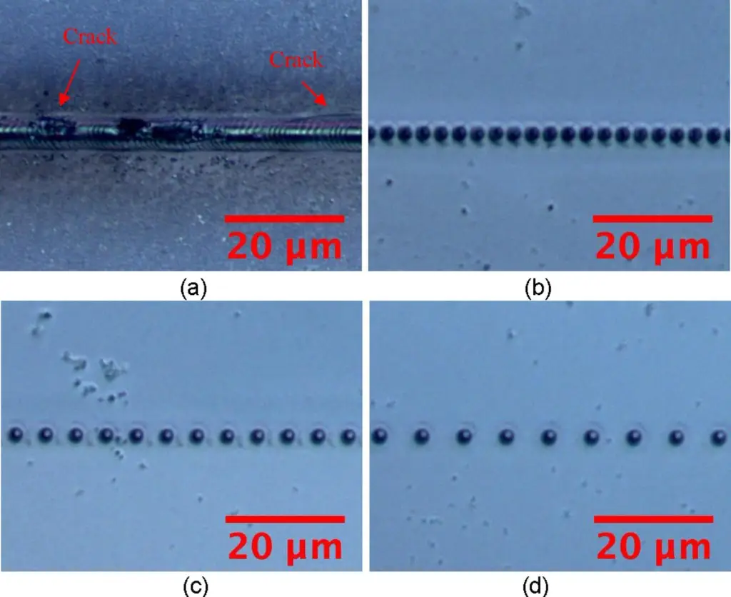
Low Speed (0.1 mm/s): High Pulse Overlap
- Large ablation area on top surface inhibits Bessel beam propagation into material
- Cracks observed within and around processing trajectory
- Heat accumulation + laser fluence → crack generation
- Sidewall structures: particles (~10 μm diameter) attached to sidewall, generally rough surface
- Re-solidification of ablated sapphire during expansion/evacuation
Medium Speed (1 mm/s): Transitional Phase
- Bessel beam pulses gradually separate; laser-irradiated areas interrupt pulse connection
- Sidewall structures: particles enlarge to ~30 μm diameter
Medium-High Speed (3 mm/s): Partial Separation
- Cracks disappear as pulses separate further
- Sidewall structures: crescent formations 40×110 μm appear
- Long axis of crescents perpendicular to Bessel beam scanning direction
High Speed (5-9 mm/s): Optimal Separation
- No unwanted structures observed
- Energy from previous pulse dissipates before next pulse arrives
- Heat accumulation reduced
- Smooth sidewall with visible trace of each Bessel beam pulse interaction
- Surface roughness: 200 nm Ra achieved
Laser Spot Characteristics:
- Measured diameter: ~1.9 μm (close to theoretical 1.8 μm central core)
- At 5-7 mm/s: slight high-order ring visible around central core (Bessel feature) but no impact on dicing quality
Material Modification Mechanism
Six-Photon Absorption Process:
- Multi-photon absorption occurs inside sapphire (high transmissivity enables internal focusing)
- Coulomb explosion and optical damage breaks electron bonds and crystalline structure
- Local pressure: ~10 TPa generated within tenths of picoseconds (sapphire → plasma transformation)
- Nano-Joule pulse energy sufficient for interior modification without damage outside focusing area
Cleavage Process:
- Three-point bending applied post-laser processing
- Support span: 35 mm between first and third points
- Motor speed: 0.01 mm/s
- Highly uniform Bessel beam + uniform material modification → zero taper cleavage
- Unirradiated areas between pulses cleave along laser scanning contour → low sidewall roughness
Thickness-Dependent Flexural Strength Results
Mechanical separation force requirements show non-intuitive thickness dependence.
Sapphire Thickness 0.38 mm:
- Flexural strength required: up to 229 MPa (highest)
- Observation: Obvious elastic bending/deformation before separation
- Explanation: Thin sheet absorbs more energy as elastic deformation before breakage
- Optimal surface roughness: achieved at 3 mm/s scanning speed
Sapphire Thickness 1 mm:
- Flexural strength required: up to 42 MPa
- Optimal surface roughness: achieved at 3 mm/s scanning speed
Sapphire Thickness 1.5 mm:
- Flexural strength required: up to 184 MPa
- Optimal surface roughness: 200 nm Ra achieved at 7-9 mm/s scanning speed
- Unexpected result: Easier to achieve low roughness for thick samples requiring higher breaking force
General Trend: Flexural strength gradually increases with scanning speed (non-linear) for all thicknesses.
Surface Quality Characterization
Measurement Methods:
- White light interferometry (Contour GT-K; Veeco): 860 μm × 650 μm measurement area
- Scanning electron microscopy (Quanta 200; FEI): 10 nm Au/Pd coating for conductivity
Crystal Orientation Independence:
- C-M 0.2° crystal orientation sapphire tested
- Two adjacent random cutting directions: 680 nm Ra and 610 nm Ra measured
- Confirmed: Crystal orientation influence on surface roughness is limited
Demonstrated Applications
Production Parameters (1.5 mm sapphire):
- Pulse energy: 450 μJ
- Scanning speed: 4 mm/s (optimized for low roughness + low bending force)
Straight Line Cutting:
- Zero taper achieved
- Debris-free
- Crack-free
- Uniform surface finish
Curved Line Cutting:
- Radius: 4 mm arcs demonstrated
- Strategy: Extra contours designed connecting arc points (0°, 45°, 90°) to reduce continuous arc length
- Result: 7 out of 10 arc points successful with straight-line prototype bending fixture
- Improvement path: Shorter-curve-shape bending fixture or additional connecting contours
Complex Geometries:
- Combination of straight lines and curves demonstrated
- Square shapes cut successfully
Key Success Factors
Achieving 200 nm Ra surface roughness requires optimization of multiple interdependent parameters:
- Bessel beam uniformity: High-purity generation via direct beam reduction through 20° axicon
- Pulse separation: Appropriate scanning speed (5-9 mm/s for 1.5 mm thickness) to eliminate heat accumulation while maintaining modification continuity
- Material thickness: Thicker samples (1.5 mm) paradoxically easier to achieve low roughness despite higher cleavage force
- Cleavage of mixed zones: Both laser-irradiated and unirradiated areas cleave together along contour
- Circular polarization: Eliminates directional distortion for omnidirectional processing
LED Manufacturing Impact
Sapphire substrate cutting quality directly impacts LED performance:
- Light extraction efficiency: Sub-micron surface roughness critical for 300-550 nm wavelength GVR LEDs
- Manufacturing yield: Zero taper ensures dimensional consistency
- Reliability: Crack-free, debris-free edges eliminate failure initiation sites
- Cost reduction: Zero kerf width maximizes substrate utilization
Comparison to Alternative Methods
This Work vs. Previous Bessel Beam Stealth Dicing:
- Surface roughness: 200 nm vs. 2000 nm (10× improvement)
- Uniformity: High vs. poor (dash-line technique eliminated)
- Crack control: Speed-based prevention vs. polarization/direction control
This Work vs. Traditional Stealth Dicing:
- Uniformity: High (entire sidewall) vs. poor (illuminated/cleaved zone mismatch)
- Surface roughness: 200 nm uniform vs. 50 nm non-uniform
This Work vs. Ablation Methods:
- Kerf width: 0 μm vs. 20-80 μm
- Debris: None vs. significant
- Taper: Zero vs. present
- Surface quality: 200 nm vs. 400-1000 nm
Technical Challenges & Considerations
Very Thin Sapphire (<0.4 mm):
- High flexural strength requirement (229 MPa) due to elastic deformation
- Alternative approaches may be more suitable: Bessel beam fracture plane generation or improved bending jig design
Curved Cutting Limitations:
- Standard straight-line bending fixtures achieve 70% success rate (7/10 arc points)
- Solution: Custom curve-matched bending fixtures or increased connecting contour density
Process Scalability:
- 1 kHz repetition rate suitable for precision but limits throughput
- Higher repetition rates would require heat accumulation management
Future Optimization Opportunities
- Higher repetition rate systems with thermal management for increased throughput
- Adaptive bending fixtures for complex curve geometries
- Multi-beam systems for parallel processing
- In-line quality monitoring via interferometry or acoustic emission
This breakthrough demonstrates that careful optimization of Bessel beam generation and pulse separation strategy can achieve surface quality approaching mechanical polishing (~200 nm Ra) while maintaining the advantages of laser stealth dicing: zero kerf, zero taper, no debris, and no cracks.
Reference: Li, Z., et al. "Stealth dicing of sapphire sheets with low surface roughness, zero kerf width, debris/crack-free and zero taper using a femtosecond Bessel beam." Optics & Laser Technology 2021, 135, 106713. https://doi.org/10.1016/j.optlastec.2020.106713
Interested in This Application?
Contact us to learn how Clear Photon workstations can enable your research or production process.
Get in Touch