Industrial Production: Precision Metal Processing with Femtosecond Lasers
Recent research published in Materials journal provides a comprehensive review of metal material processing using femtosecond lasers, demonstrating transformative capabilities across drilling, surface modification, printed circuit board (PCB) micromachining, and liquid metal processing.
Why Femtosecond Lasers Excel at Metal Processing
Unlike traditional long-pulse lasers, femtosecond lasers enable 'cold ablation': a fundamentally different processing regime:
- Ultrashort pulses: Operating at 10⁻¹⁵ seconds, the pulse duration is significantly shorter than the material's heat diffusion time.
- Direct solid-to-plasma conversion: Material is removed via rapid conversion into plasma before thermal diffusion can affect the surrounding lattice.
- Minimal HAZ: The heat-affected zone (HAZ) is typically sub-micron, a stark contrast to the massive thermal spread typical of nanosecond lasers.
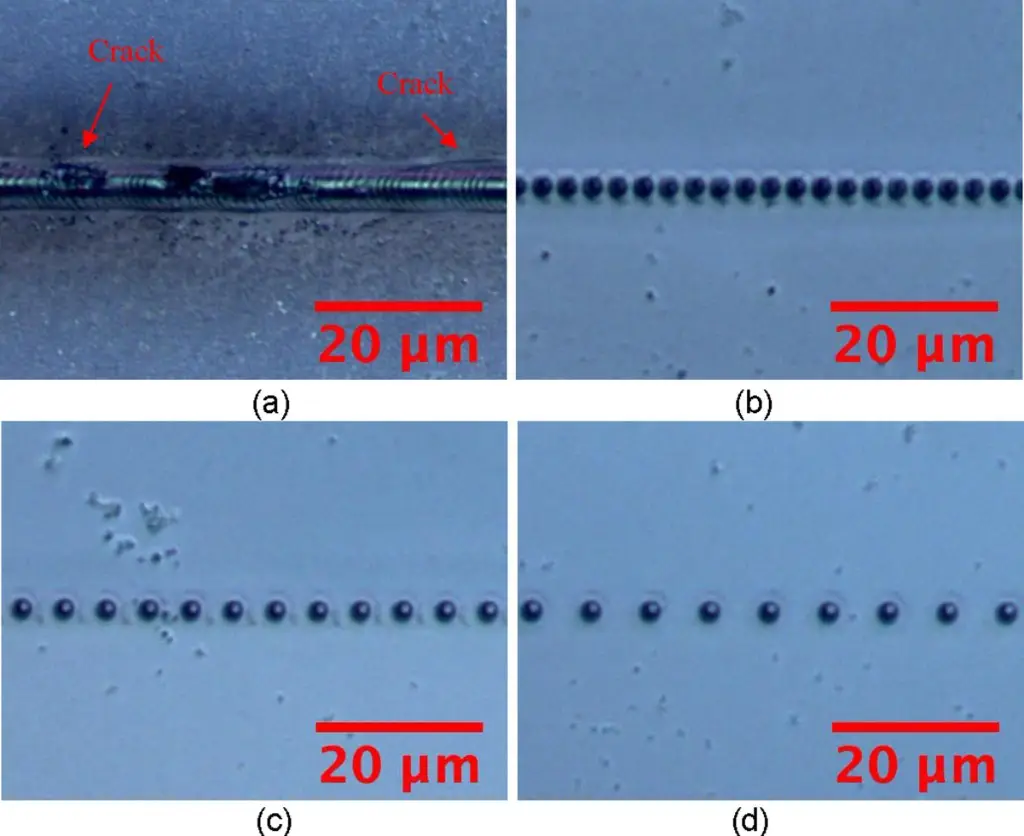
- No thermal damage: The process avoids microcracks, remelting, or damaging thermal expansion effects.
This 'cold processing' characteristic makes femtosecond lasers ideal for precision metal applications that demand zero thermal damage.
Precision Metal Drilling: Refractory Materials
Femtosecond lasers have become the preferred method for high-precision drilling of difficult-to-machine metals, including refractory metals with extremely high melting points.
Key Research Findings:
- Ti-6Al-4V ablation threshold: Precisely measured at 0.29 J/cm² by Xu et al.
- Stainless steel 304 threshold: Measured at 0.077 ± 0.008 J/cm² at low fluence and 0.46 ± 0.05 J/cm² at high fluence.
- Tungsten drilling: Zhang et al. demonstrated high-quality holes with smooth walls and no HAZ, even after exposure to 4 × 10⁶ pulses.
- Ti6Al4V optimal parameters: Deepu et al. found that optimal hole quality is achieved at 0.44 J/cm², 10 kHz, and an 85% pulse overlap.
Advanced Drilling Strategies:
- Two-stage pulse energy (TSPE): Zhang et al. successfully minimized hole taper by utilizing a 40 μJ initial stage followed by a 50 μJ second stage.
Ablation Threshold Physics
The ablation threshold represents the minimum energy density required for material removal.
Multi-Metal Ablation Data (Genieys et al., 800 nm, 15–100 fs):
- Aluminum: Maintains a consistent ablation threshold across varying ultrafast pulse durations.
- Copper: Its naturally high reflectivity is successfully compensated for by nonlinear absorption mechanisms.
- Nickel & Tungsten: Show ultra-stable ablation thresholds independent of pulse duration in the ultrafast regime.
Critical Finding: For all tested metals, the ablation threshold remained constant across 15–100 fs pulse durations, confirming that the ultrafast regime operates on fundamentally different physics than longer pulses.
Micro/Nano Surface Modification
Femtosecond laser surface modification enables the creation of functional micro/nano structures impossible with conventional methods.
Laser-Induced Periodic Surface Structures (LIPSS):
- Formation mechanism: Self-organized periodic structures emerge when laser intensity is maintained slightly above the ablation threshold.
- Applications: These structures can induce structural colors, anti-reflection properties, and controlled wettability.
Industrial Applications Demonstrated:
- Fe-Cr-Al resistor trimming: Su et al. proved femtosecond lasers offer higher precision than nanosecond lasers due to lower single-pulse energy and reduced thermal effects. Bulk metallic glass coloring: Gao et al. demonstrated that Zr-based BMG changes from yellow to brown to green as energy density increases from 0.5 to 8.0 J/mm².
- Microgroove fabrication: Liang et al. utilized spatial beam shaping to create deep grooves (10–150 μm width) with no HAZ.
Surface Enhancement Results:
- Microhardness: Surface microhardness of Ti6Al4V improved by 16.6% at 150 μJ laser energy.
- Residual stress: Induced a maximum residual compressive stress of 746 MPa, significantly enhancing fatigue resistance.
Printed Circuit Board (PCB) Micromachining
Femtosecond lasers enable precision PCB processing that conventional methods cannot achieve.
PCB Repair & Fabrication:
- Circuit repair: Lim et al. used Femtosecond Laser Direct Writing (FsLDW) to create conductive reduced graphene oxide (rGO) traces, repairing damaged copper tracks.
- High-precision patterning: Lu et al. achieved copper tracks with 15–65 μm pre-defined widths and an outstanding machining accuracy of ~0.67 μm.
- Reverse engineering: Choi et al. combined automated layer-by-layer ablation with digital microscope imaging to capture internal PCB structures more accurately than X-ray CT.
Optimal Processing Parameters (Tao et al.):
- Using 100 mW etching power, 10 mm/s speed, and a 4 μm groove gap, researchers produced a compact 1×16 polymeric optical splitter with insertion loss ≤ 20 dB.
Liquid Metal Processing for Flexible Electronics
Femtosecond laser surface modification unlocks breakthrough capabilities in manipulating liquid metal (LM) for flexible electronics.
Liquid Metal-Repellent Surfaces:
- Technology: Chen's team used an 800 nm femtosecond laser to create microstructures on PDMS exhibiting supermetalphobicity to Ga-based liquid metals (contact angle > 150°, sliding angle < 10°).
Magnetic Liquid Metal (MLM) Circuit Printing:
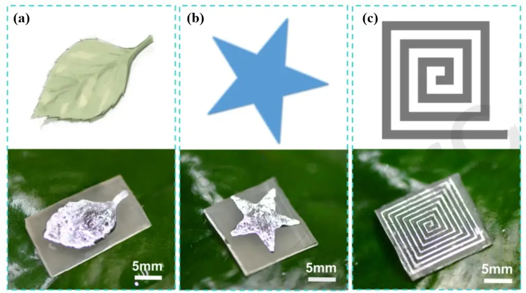
- Wu et al. created a supermetalphobic silicone surface (contact angle 169.5° ± 3.5°) where a magnetic field guides MLM droplets to print and repair flexible circuits.
All-Flexible Tactile Sensor:
- Zhang et al. developed a sensor using a double-sided micropyramid dielectric layer and an LM electrode, achieving a pressure sensitivity of 2.78 kPa⁻¹, detection limit of ~3 Pa, an 80 ms response time, and a durability exceeding 10,000 cycles.
Future Outlook & Industrial Challenges
While femtosecond laser metal processing offers unprecedented capabilities, integrating it at an industrial scale presents unique hurdles. Current challenges include refining multi-pulse two-temperature models for high-repetition-rate cumulative effects, managing heat accumulation at MHz frequencies, and scaling up laboratory-stage discoveries to commercial deployment.
However, with the advent of accessible desktop systems and Class 1 safety enclosures, this technology is rapidly democratizing. As hybrid approaches combining nonlinear optics and chemical etching mature, femtosecond micromachining will continue to redefine manufacturing possibilities in aerospace, medical implants, and flexible electronics.
Reference: He, Z., et al. "Metal Material Processing Using Femtosecond Lasers: Theories, Principles, and Applications." Materials 2024, 17(14), 3386. https://doi.org/10.3390/ma17143386
Interested in This Application?
Contact us to learn how Clear Photon workstations can enable your research or production process.
Get in Touch